
Work Plan
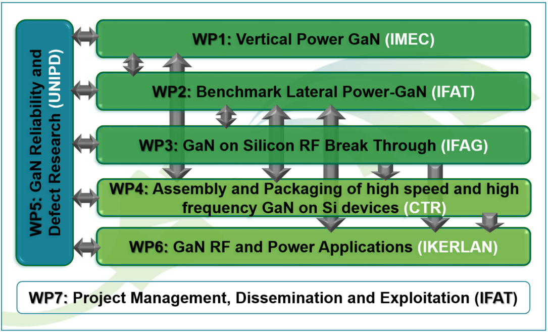
The ambitious project objectives towards next-generation GaN technologies require a holistic approach in terms of novel technologies being linked to assembly and packaging efforts and accompanied by reliability and defect research to finally fit to the related power applications.
The cooperation model is well aligned with achieving the overall UltimateGaN objectives and ideally supports the entire supply chain to foster the digitalisation attempts. All necessary aspects are combined by following a classical work package structure with 7 work packages that are closely connected to each other.
WP1 Vertical Power GaN
WP leader: IMEC
WP partners: CTR, IMEC, AIX, MPIE, Fraunhofer, NaMLab, UNIPD, STUBA, RISE
In WP1 a vertical device technology will be developed on large area (200mm) substrates with CMOS compatible process modules. To enable high voltage operation of these switches, an epi stack with a thick drift region will be developed on the novel CTE matched substrate poly-AlN, the drift region will have a minimum thickness of 5µm. Further activities will support this overall objective, i.e. design and simulation of the material and switches and detailed material characterization of the stack and fabricated components. Reaching this objective will be a real breakthrough for vertical GaN devices, enabling a cost effective path for high voltage switches and a potential contender for SiC switches. In parallel to the work on large area substrates vertical devices with thick drift layer on 2” GaN substrates will be fabricated for exploring the material limit and benchmarking purpose.
This is directly in line with the overall project objective 1 of exploring the path towards vertical power GaN devices and related technologies. By investigating novel materials, thick drift region and large area CMOS compatible processing we will work towards a first large scale manufacturable vertical GaN device technology.
WP2 Benchmark Lateral Power GaN
WP leader: IFAT
WP partners: IMEC, AIX, IFAG, MPIE, Fraunhofer, EPFL, ATT, RISE, SweGaN
This work package focuses on the realization of high-voltage (600V) normally-off lateral GaN power HEMTs on 200mm wafer diameter with a drastically improved performance to cost ratio compared to state-of-the-art devices. Beside the development of an enabling high-quality and low-cost 200mm GaN on Si epitaxy, a main objective will be a die shrink by minimizing both non-active die areas and active GaN transistor cells together with an optimization of the interconnect scheme. In order to reach out to the limits beyond existing pGaN concepts, most innovative lateral HEMT approaches with revolutionary figure-of-merits will be explored.
In addition, low voltage (100V) lateral GaN power HEMT technology will be brought to the next stage of maturity regarding performance and reliability to empower ground breaking innovations in automotive LIDAR applications, in which the unrivalled fast switching of GaN HEMT devices will be vital.
Finally, a path will be explored in which buffer-free GaN on SiC epitaxy wafers with dislocation density and crystal quality levels not achievable with GaN on Si shall be realized in a cost competitive approach, and nano-wire based GaN on Si buffers (initially on 2” substrates) will be produced for benchmarking purposes.
The best-in-class lateral GaN power devices developed in this work package will enable the next levels of power density and efficiency in many applications. The strongly improved performance to cost ratio lays the foundation for the broad adoption of GaN power HEMTs made in Europe in cost competitive and growing markets. If widely used, GaN based power electronics will have a strong positive effect on energy and material efficiency for European as well as global economies and societies.
WP3 GaN on Silicon RF Break Through
WP leader: IFAG
WP partners: IFAT, AIX, SAG, Fraunhofer
Within work package WP3 the development of a base technology platform for 4,5GHz and 28 GHz of a normally-on lateral GaN HEMT mm Wave MMIC device will be addressed and demonstrated. This is including the complete development chain. Starting with the Concept Selection for the 28 GHz device; technology development of the needed process blocks and single processes and EPI processes; performance optimization by using advanced processes and methods like 100nm gate foot length and special gate geometries; Robustness & Reliability evaluations and improvements addressing among other things RdsON and Vth Drifts, and ending finally with a functional and measurable 28 GHz device to demonstrate the performance and capabilities of this new technology platform.
With the development of this technology and its processes compatible to a standard high volume 200mm wafer manufacturing silicon CMOS and power fab, we will drive the technology knowledge and manufacturability in Europe to a best in class status with respect to power density and efficiency, and increase the market share of RF and Power applications made in Europe.
WP4 Assembly and Packaging of high speed and high frequency GaN on Si devices
WP leader: CTR
WP partners: IFAT, TUGraz, AT&S, IFAG, RISE
This work package includes research on assembly and packaging for high frequency GaN on Si devices. GaN on Si devices can only be successful in case a proper packaging technology is available which reaches the application specific performance targets (low parasitic effects, high frequency and heat dissipation capabilities), miniaturization and system integration capabilities at acceptable costs and reliability (link to WP5). Thus, this work package focuses on three different applications related to three objectives with different high frequency constraints where GaN on Si chips have outstanding potential. The WP4 partners will investigate technological paths to solve the current limitations of electrical interconnects, cooling and dynamic performance in terms of peak currents and high frequencies. The technology investigations will always take the reliability aspect into account, crucial to package the brittle GaN on Si devices. The work package has a strong influence on the overall device performance and thus, contributes to the overall project objectives. The trade-off between performance, reliability and cost will be investigated and the outcome will be a performance matrix in respect to applications (see Table 2, D4.6).
WP5 GaN Reliability and Defect Research
WP leader: UNIPD
WP partners: IFAT, Fronius, TUGraz, AT&S, IMEC, AIX, IFAG, MPIE, Fraunhofer, TUC, Eltek, STUBA, Nano, ATT, IKERLAN, 4Fores, LEAR
WP5 focuses on the analysis of performance and reliability-limiting mechanisms in advanced GaN devices. Specific focus will be on defect characterization, since point and extended defects can limit the dynamic performance, breakdown voltage and the long-term stability of GaN transistors. The results will provide inputs to WP1-WP3 for the improvement of vertical devices, lateral devices and GaN on Si RF transistors, to WP4 for the development of advanced packaging strategies, and to WP6 on application-level reliability. Specific tests will be carried out at material, device and system level, to cover the full value chain.
WP6 GaN RF and Power Applications
WP leader: IKERLAN
WP partners: IFAT, Fronius, TUGraz, IFAG, IFI, UniMiB, Eltek, 4Fores, LEAR
The objective of this work package is to evaluate and quantify the benefits of the new developed devices in real RF and power applications. By the use of these devices, the RF power amplifiers and power converters will achieve several improvements on system performance, such as higher efficiencies, higher power densities and/or higher operation frequencies. The chosen highly benefitting applications are next generation rectifiers for telecom and data centres; solar PV inverters; isolated power converters for native DC microgrids; nano-second-pulsed-laser-driver for LIDAR; battery charger for PHEV/EV; and power amplifiers for RF frontends for 5G and radar applications.
One of the key in WP6 will be to find the optimal design in each application to take full advantage of the GaN benefits (i.e. no low recovery charges, fast commutations, low switching losses, low conduction resistance, low gate charges) and to handle the main challenges of the new technology (i.e. high dv/dt values, thermal management methods, high-frequency inductive elements, control strategies, fast protection systems...). The developed prototypes in WP6 have to demonstrate the potential of the project GaN devices to significantly improve the system performance in each Use Case.
WP7 Project Management, Dissemination and Exploitation
WP leader: IFAT
all project partners contribute
This work package is split into three main objectives: (1) Management and Risk Mitigation; (2) Dissemination; (3) Exploitation. The project will be led by Infineon Technologies Austria AG (IFAT), overseeing the technical content as well as the administration to manage resources and results according to the project plan and thus ensuring exploitation. These tasks are supported by a team of highly experienced people with controlling, financial and legal backgrounds. In WP7 the project coordinator will closely work together with the dissemination leader in order to also properly spread the project results among diverse stakeholder groups and communities in Europe.